Table of Contents
What is opamp?
Opamp Definition :
An opamp is considered as a very high gain differential amplifier that is capable of performing the mathematical operation of division, multiplication, addition, subtraction, differentiation & integration.
Block diagram of an OP-amp

fig1.Block diagram of a typical op-amp
Input Stage:- This stage comprises of a dual input balanced output differential amplifier. Dual input means it requires two input terminals and the differential amplifier function is to amplify the difference between the two input signals. This stage delivers most of the amplifier’s voltage gain and requires high input impedance to avoid loading on the sources.
Intermediate Stage:-This stage is a dual input, unbalanced output(single-ended output) differential amplifier. Opamp has a very high overall gain requirement that cannot be provided by the input stage alone. So the main purpose of the intermediate stage is to provide the additional voltage gain required. This stage increases the overall gain of the opamp.
Level Shifting Stage: As opamp amplifies dc signal, stage by stage dc level increases well above the ground potential such a high dc may cause the transistor to saturate. This further may cause distortion in the output due to clipping. So to avoid output distortion, we place a level shifter just before the output stage to shift the dc level of the output of the intermediate stage down to zero volts with respect to the ground. Usually, this stage comprises of emitter follower whose impedance is very high.
Output stage: -The basic need of an output stage are low output impedance, large a.c output voltage swing, and high current sourcing and sinking capability. The push-pull complementary amplifier fulfills all these requirements and is hence used as an output stage.
Circuit symbol Of Opamp

Fig2. The circuit symbol of Op-amp
• An opamp has two input terminals:
1.One terminal is labelled as “-” is known as Inverting input terminal. The word inverting means that if a signal is applied to this terminal, it appears at the output with 180o phase shift or opposite polarity.
2.The other terminal labelled as “+” is known as a non-inverting input terminal. The word non-inverting means that if a signal is applied to this input, it appears at the output without any phase shift.
• It has two power supplies: Positive power supply(+V or +Vcc) and Negative power supply(-V or -VEE) of equal magnitude but opposite polarity.
•It has one output terminal.
Equivalent Circuit of an Op-amp

Fig3. Equivalent circuit of Op-amp
The output section consists of a voltage-controlled source in series with the output resistance Ro. The input resistance Ri is the Thevenin equivalent resistance seen at the input terminal, while the output resistance Ro is seen at the output.
The differential input voltage Vid is given by
{\displaystyle V_{id}\;=V_1\;-\;{V_2}}
where V1=Voltage between Non-inverting terminal and ground.
V2=Voltage between inverting terminal and ground.
The output voltage Vo is given as
{\displaystyle V_o\;=A_d\;V_d\;=A_d\;(V_1\;-V_2)}
where Ad is called open-loop voltage gain.
Op amp Characteristics
Opamp Differential Gain(Ad)

Fig4. Differential Gain
The output Voltage Vo of the differential amplifier is given as
{\displaystyle V_o\;=A_d\;(V_1\;-V_2)}
{\displaystyle V_o\;=A_d\;V_d}
So , {\displaystyle A_d\;=\frac{V_o}{V_d}}
In decibel differential gain is given as
A_d=\;20\;\log_{10}\;(A_d)\;in\;dB
where Ad is the gain with which differential amplifier amplifies the difference between two input signals. Hence it is called as a differential gain of the differential amplifier.
Opamp Common Mode Gain
The output of the practical differential amplifier not only depends on the difference voltage but also depend on the average common level of the two inputs which is called a Common mode signal (Vc) given as
{\displaystyle V_{c\;\;}=\frac{V_1\;+V_2}2}
The output voltage due to common mode signal Vc is {\displaystyle V_o\;=\;A_c\;V_c}
Where , Ac is common mode gain
So , The total output of any differential amplifier is given as
{\displaystyle V_o\;=\;A_d\;V_d\;+\;\;A_c\;V_c}
Opamp Common Mode Rejection Ratio(CMRR)
It is defined as the ratio of differential voltage gain Ad to common-mode voltage gain Ac
so, {\displaystyle CMRR}\;=\;\left|\frac{\displaystyle A_d}{\displaystyle A_c}\right|
CMRR can be expressed in dB as,
{\displaystyle CMRR\;in\;dB\;=20\;\log\;\left|\frac{A_d}{A_c}\right|\;dB}
Opamp Slew Rate
It is defined as the maximum rate of change of output with respect to time. It is expressed in {\displaystyle V/\mu s}
{\displaystyle Slew\;Rate(SR)\;={\left.\frac{dV_0}{dt}\right|}_{max}}
It’s ideal value is infinite for the op-amp
Opamp Input offset voltage

Fig.5 Input Offset Voltage
In an ideal opamp, the output should be zero when both the inputs are grounded. But due to certain imbalances in the circuitry, in all practical opamps, there has to be some differential input to give a zero output. This small differential input is called as input offset voltage given as,
{\displaystyle V_{io}}\;=\;{\displaystyle V_{dc_1}}\;+\;\;{\displaystyle V_{dc_2}}
Where {\displaystyle V_{dc_1}\;\&\;V_{dc_2}} are dc voltages.
Opamp Input Offset Current

Fig6. Input offset current
For ideal opamps, the input bias current IB1 and IB2 should be equal. In practice, these currents are not equal because of the internal imbalances in the opamp circuitry. The algebraic difference between the current into the inverting and noninverting terminals is called as input offset current given as
Input offset current , {\displaystyle I_{io\;}=\left|I_{B1\;}-I_{B2}\right|}
Opamp Bias Current
Input bias current IB is the average of the current that flows into the inverting & Noninverting terminals of the opamp given as,
Bias current , {\displaystyle I_{B\;}=\frac{I_{B1\;}+I_{B2}}2}
where IB1 = Input bias current for inverting terminal.
IB2= Input bias current for Noninverting terminal.
Opamp Power Supply Rejection Ration(PSRR)

Fig.7 power supply rejection ratio
It is defined as the ratio of change in input offset voltage due to the change in supply voltage producing it , keeping other power supply voltage constant.
so , for a fixed VEE
{\displaystyle PSRR={\left.\frac{\triangle V_{io}}{\triangle Vcc}\right|}_{V_{EE\;Constant}}}
For a fixed Vcc,
{\displaystyle PSRR={\left.\frac{\triangle V_{io}}{\triangle V_{EE}}\right|}_{V_{CC\;Constant}}}
Ideal Opamp
Definition: An ideal opamp is an amplifier with infinite open-loop gain, Infinite input Resistance, and zero output resistance.
Characteristic of Ideal Opamp
- Infinite open loop gain (AOL=∞)
- Infinite input impedence(Rin=∞)
- Zero output Impedence(RO=0)
- Zero offset Voltage(Vio=0)
- Infinite Bandwidth (BW=∞)
- Infinite Slew Rate(SR=∞)
- Infinte CMRR (ρ=∞)
- Zero Power Supply Power Rejection Ratio (PSRR=0)
Equivalent circuit of Ideal op-amp
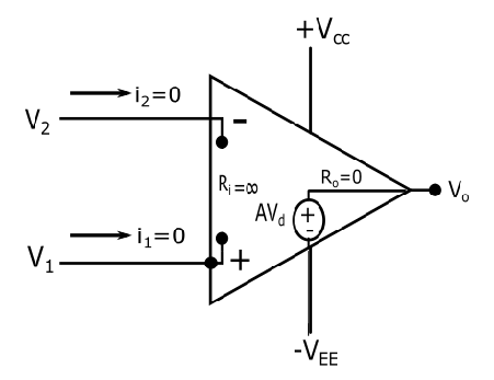
Fig8. Ideal opamp
- An ideal opamp does not draw the input current because the input resistance of an ideal opamp is infinite(Ri = ∞ ).
- For an ideal opamp , output resistance Ro=0 , so it is replaced by a short circuit in the output portion of equivalent circuit.
Ideal Opamp Voltage Transfer Curve

Fig 9. Ideal Opamp Voltage Transfer Curve
Definition: A Voltage transfer Curve may be defined as a curve that is drawn between input and output voltages. for op-amp the input voltage is Vd and the output is Vo.
The practical limitation of the op-amp is that the magnitude of the output voltage cannot exceed |Vcc| or |V|. The Op-amp can operate in three modes, depending on the differential input voltage Vd
- Positive saturation Vo= Vcc
- Linear Region -VEE ≤ Vo≤Vcc
- Negative Saturation Vo=-VEE
If we increase Vd beyond the linear range then the op-amp becomes saturated and output V0 = -VEE or V0 = +Vcc.
Inverting Amplifier
Definition:– An op-amp circuit that produces an amplified output signal that is 180° out of phase with the input signal.
Circuit Diagram
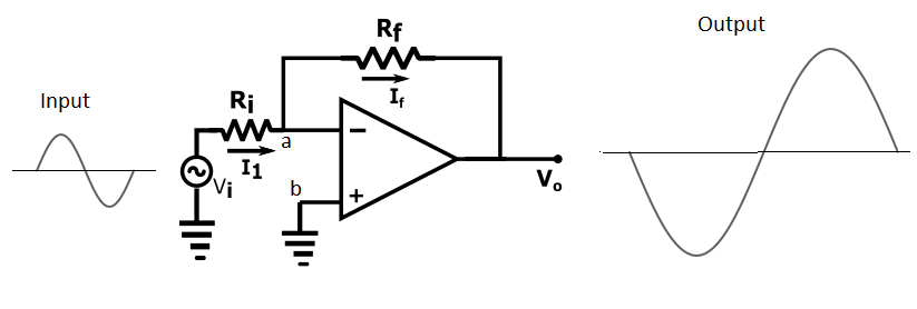
Fig 10. Inverting Amplifier
In this circuit, the non inverting terminal is grounded ,input voltage Vi is applied to the inverting terminal through resistance Ri , Rf is the feedback resistance connected between inverting input and output terminals.
Expression for output voltage Vo
From fig 10 , Apply KCL at node a.
{\displaystyle I_1}={\displaystyle I_f} ………………………….(1)
Here input current {\displaystyle I_1=\frac{\displaystyle V_i-V_a}{\displaystyle R_i}} …………………(2)
output current {\displaystyle I_ f\;}=\frac{\displaystyle V_a-V_o}{\displaystyle R_f} …………………(3)
putting the value of equation (2) & (3) in equation (1) we get
\frac{\displaystyle V_i-V_a}{\displaystyle R_i}=\frac{\displaystyle V_a-V_o}{\displaystyle R_f} …………………(4)
But {\displaystyle V_a}={\displaystyle V_b}={\displaystyle 0} (Due to virtual ground concept)
So, putting the value of Va in Eqn(4) we get
\frac{\displaystyle V_i-0}{\displaystyle R_I}=\frac{\displaystyle 0-V_O}{\displaystyle R_f}
Hence, \frac{\displaystyle V_i}{\displaystyle R_I}=\frac{\displaystyle -V_O}{\displaystyle R_f}
The output voltage of inverting amplifier can be given as
{\displaystyle V_O}=-\frac{\displaystyle R_f}{\displaystyle R_I}V_i
The voltage gain of the inverting amplifier is given by
{\displaystyle A_v}=\frac{\displaystyle V_O}{\displaystyle V_i}=-\frac{\displaystyle R_f}{\displaystyle R_I}
Concept Of Virtual Ground

Fig11. Virtual ground Concept
A point in any circuit is said to be grounded if the potential at that point is equal to the ground potential. In the case of virtual ground, the potential at that point becomes the same as ground potential but physically no path for current from that point to the ground exists.
For opamp, we know that
Gain {\displaystyle A}=\frac{\displaystyle V_o}{\displaystyle V_d}
{\displaystyle V_d}\;={\displaystyle V_2}\;-\;{\displaystyle V_1}
Therefore A\;=\frac{\displaystyle V_0}{\displaystyle V_2-V_1}
{\displaystyle V_2-V_1}=\frac{\displaystyle V_0}A
{\displaystyle V_2-V_1}\;=\frac{\displaystyle V_0}\infty=0 (for ideal opamp A=∞)
so {\displaystyle V_2=V_1}\;
In the above circuit V2 = 0
V1 =V2 =0
V1 = 0 due to virtual ground.
Non Inverting Amplifier
Definition:- An opamp circuit that produces an amplified output that is of the same phase. The input is applied directly to the noninverting terminal.
Circuit diagram

Fig 12. Noninverting Amplifier
Expression for output voltage and Gain
In the above circuit, apply KCL at node a, we get
{\displaystyle I_f}\;={\displaystyle I_1}\;\;\;\;\;\;\;\Rightarrow\;\;\frac{\displaystyle V_O-V_a}{\displaystyle R_f}\;\;\;=\frac{\displaystyle V_a-0}{\displaystyle R_1}\;\;\;........................\;\;(1)
But V_a-V_{in}\;\;\;\;\;\;\;\;\;\;\;\;\;\;\;\;............................\;\;(2)
Put Eqn (2) in Eqn (1) we get ,
so , \;\;\frac{\displaystyle V_O-V_i}{\displaystyle R_f}\;\;\;=\frac{\displaystyle V_i}{\displaystyle Ri}\;\;\;\;\;\;\;\;\;\;\Rightarrow\;\;\;\frac{\displaystyle V_O}{\displaystyle R_f}\;-\frac{\displaystyle V_i}{\displaystyle R_f}\;=\;\frac{\displaystyle V_i}{\displaystyle R_i}
Therfore, \frac{\displaystyle V_o}{\displaystyle R_f}=\;\frac{\displaystyle Vi}{\displaystyle R_i}\;+\;\frac{\displaystyle V_i}{\displaystyle R_f}\;\;\;\;\;\;\;\;\;\;\;\Rightarrow\;\;\;\;\;\;\;\frac{\displaystyle V_o}{\displaystyle R_f}=V_{in}\left(\frac{\displaystyle1}{\displaystyle R_i}+\frac{\displaystyle1}{\displaystyle R_f}\right)
{\displaystyle V_o}\;={\displaystyle V_{in}}\;\left(1+\frac{\displaystyle R_f}{\displaystyle R_i}\right)
The gain of non inverting amplifier is given by
{\displaystyle A_v}\;=\frac{\displaystyle V_o}{\displaystyle V_{in}}\;=\;1+\frac{\displaystyle R_f}{\displaystyle R_i}
Opamp Voltage follower / Unity gain amplifier /Buffer Amplifier
Definition: A Voltage follower is an opamp circuit in which output follows the input. It is also called Unity gain buffer amplifier.
Circuit diagram
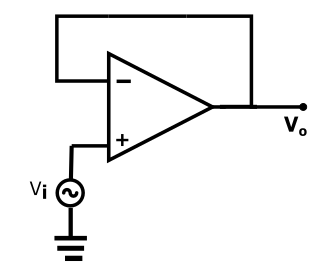
Fig 13. Voltage follower
The Voltage follower is a special case of a Non-inverting amplifier.
The gain for the Non-Inverting amplifier is
{\displaystyle A_v}\;=\frac{\displaystyle V_o}{\displaystyle V_{in}}\;=\;1+\frac{\displaystyle R_f}{\displaystyle R_i}\;\;\;\;\;\;\;\;\;\;\;\;.............................(1)
Now , let Rf = 0 (short circuit)
Ri = ∞ (open circuit)
Substituting these two condition in Eqn (1) , we get,
{\displaystyle A_v}\;=\;1+0=\;1
Since the gain of the amplifier is 1(unity), so it is known as a Unity gain amplifier.
\frac{\displaystyle V_o}{\displaystyle V_{in}}\;=\;1
or {\displaystyle V_o}\;=\;{\displaystyle V_{in}}
According to the above equation, the output of the voltage follower is equal to the input all the time.
Opamp Applications
An Opamp has many applications such as it can be used as
- Adder or Summer
- Integrator
- Differentiator
- Differential Amplifier or Difference Amplifier.
Opamp Summer or adder
Definition: An adder is an op-amp circuit, that can accept two or more inputs and produces output as the sum of these inputs.
Circuit diagram

Fig 14.Three input adder.
Expression for Output Voltage
Let three voltages Va, Vb, Vc are applied to the inverting input of the opamp.
Apply KCL at node A, we get,
{\displaystyle I_a}\;+\;{\displaystyle I_b}\;+\;{\displaystyle I_c}\;=\;{\displaystyle I_f}\;\;\;\;\;\;\;\;\;\;\;\;\;\;\;\;\;\;\;\;\;\;\;\;\;\;\;\;...................................\;(1)
The output Voltage is given as
{\displaystyle V_o}\;=\;-{\displaystyle I_f}\;{\displaystyle R_f}=-{\displaystyle R_f}\;\left({\displaystyle I_a\;+\;I_b}\;+\;{\displaystyle I_c}\right)\;\;\;\;\;\;\;\;\;\;\;\;\;\;\;\;.......................................(2)
Also , {\displaystyle I_a}\;=\frac{\displaystyle V_a}{\displaystyle R_1}\;\;,\;\;\;\;\;\;\;\;I_b\;=\;\frac{\displaystyle V_b}{\displaystyle R_2}\;\;\;\;\;\;\;\;\;\;\;\;\;\;\;{\displaystyle I_c}\;=\frac{\displaystyle V_c}{\displaystyle R_3}
Putting all these values in Eqn (2) we get ,
{\displaystyle V_o}\;=-\;{\displaystyle R_f}\;\left(\frac{\displaystyle V_a}{\displaystyle R_1}+\;\frac{\displaystyle V_b}{\displaystyle R_2}+\frac{\displaystyle V_c}{\displaystyle R_3}\right)
If\;R_1\;=R_{2\;}=R_3\;=R_f\;=R\;then\;we\;have
{\displaystyle V_o}\;=-\;{\displaystyle R}\;\left(\frac{\displaystyle V_a}{\displaystyle R}+\;\frac{\displaystyle V_b}{\displaystyle R}+\frac{\displaystyle V_c}{\displaystyle R}\right)
{V_o}\;=-\;(\;{V_a+V_b+V_c})
Therefore , output is equal to the sum of three input voltages.
Opamp Integrator
Definition: An Integrator is a circuit in which the output voltage waveform is the integral of the input voltage waveform.
Circuit Diagram
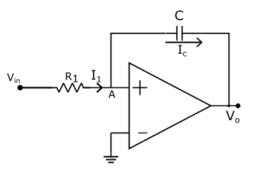
Expression for Output voltage
Because of the virtual ground and infinite input impedance of the Opamp, all of the input current I1 flows through the capacitor.
so \;\;\;\;_{\displaystyle I_1\;=\;I_c}
Now , input current {\displaystyle I_1}\;=\;\frac{\displaystyle V_{in}\;-0}{\displaystyle R_1}\;=\frac{\displaystyle V_{in}}{R_1}\;\;\;\;\;\;\;\;\;\;\;\;\;\;\;\;\;\;\;\;\;\;\;\;\;\;\;\;\;...............................\;\;\;(1)
Also, Voltage across the capacitor is
{\displaystyle V_c}\;=\;{\displaystyle 0-V_o}\;=\;{\displaystyle -V_o}
{\displaystyle I_c\;=\;C\frac{dV_c}{dt}\;=\;-C\frac{dV_o}{dt}}\;\;\;\;\;\;\;\;\;\;\;\;\;\;\;\;\;\;\;\;...................................\;\;(2)
From Eqn (1)and (2) we get,
{\displaystyle \frac{V_in}{R_1}\;\;\;=\;- C\frac{dV_o}{dt}}\;\;\;\;\;\;\;
integrating both sides and rearranging the equation we get,
{\displaystyle V_o}=\;\frac{\displaystyle -1}{\displaystyle R_1C}\int_0^tV_{\displaystyle in}\;{\displaystyle dt}
It is clear from the above equation that output voltage is proportional to the integration of input voltage.
Opamp Differentiator
Definition:- A differentiator is a circuit in which the output voltage waveform is the differential of the input voltage waveform.
Circuit Diagram

Expression for output voltage
Due to the Virtual ground concept and infinite input impedance same current flows throw the capacitor and feedback resistance
So,{\displaystyle I_c}\;={\displaystyle I_f}\;\;\;\;\;\;\;\;\;\;\;\;.............................(1)
The current through the capacitor can be given as
{\displaystyle I_c}\;={\displaystyle C}\;\frac{\displaystyle dV_{in}}{\displaystyle dt}\;\;\;\;\;\;\;\;\;\;\;\;.............................(2)
The current through the feedback resistance can be given as,
{\displaystyle I_f}\;=-\frac{\displaystyle V_o}{\displaystyle R_f}\;\;\;\;\;\;\;\;\;\;\;\;.............................(3)
Now putting Eqn (2) & (3) in Eqn(1) we get,
{\displaystyle C}\;\frac{\displaystyle dV_{in}}{\displaystyle dt}=-\frac{\displaystyle V_o}{\displaystyle R_f}
{\displaystyle V_o}={\displaystyle -R}_{\displaystyle f\;}{\displaystyle C}\;\frac{\displaystyle dV_{in}}{\displaystyle dt}
Therefore, It is clear from the above equation that the output voltage is proportional to the differentiation of input Voltage.
Opamp subtractor / Difference Amplifier / Differential Amplifier
Definition:- A differential Amplifier is a circuit that amplifies the difference between two input voltages. For a differential amplifier, Voltages are applied at both the op-amp input terminals i.e inverting & Non inverting terminals.
Circuit diagram

Expression for output Voltage
The differential amplifier can be analyzed with the help of the superposition principle. So,
Case I : Reducing VB to zero
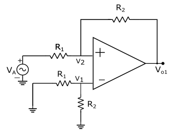
Now the equivalent circuit has been converted into Inverting Amplifier.
So,{\displaystyle V_o}={\displaystyle -}\;\frac{\displaystyle R_2}{\displaystyle R_1}\;{\displaystyle V_A}
Case II : Reducing VA to Zero

Now the equivalent circuit of Fig.17 has converted into Non inverting Amplifier as shown below
So by using the potential divider rule we get
{\displaystyle V_1=V_B}\;\times\;\frac{\displaystyle R_2}{\displaystyle R_1+R_2}
The output voltage is given as
{\displaystyle V_{02}=V_1}\;\left(1+\frac{\displaystyle R_2}{\displaystyle R_1}\right)\;\;=\;\;{\displaystyle V_B}\;\frac{\displaystyle R_2}{\displaystyle R_1+R_2}\left(\frac{\displaystyle R_1+R_2}{\displaystyle R_1}\right)
The overall output is the sum of case I and case II output as given below:
{\displaystyle V_o}\;=\;{\displaystyle V_{o1\;}+V_{02}}
{\displaystyle V_o=-\frac{R_2}{R_1}\;V_A\;\;+\;\frac{R_2}{R_1}\;V_B}
{\displaystyle V_o=\;\frac{R_2}{R_1}(V_B-\;V_A)}
Therefore from the above equation, it is clear that the output is proportional to the difference of the input voltage
After reading this article on Opamp you can check your understanding of this topic by solving MCQ on Opamp.
Suggested Article from Wisdom Imbibe:


Useful