Table of Contents
Digital to Analog Converter (DAC)
Definition
A digital to analog converter is a device that is used to transform analog signals into digital signals.
Basic DAC techniques
The schematic diagram of DAC is shown below in fig 1.

The DAC has an n bit binary word as an input that is combined with reference voltage VR to produce an analog output voltage Vo. Mathematically DAC output can be given as
Vo = K VFS (D12-1 + D22-2 +D32-3 +……….+Dn2-n)
Where Vo = output Voltage
VFS= Full-scale output voltage when all binary inputs are 1.
K= Scaling Factor generally set to unity
D1D2……Dn = n bit binary input.
D1 = Most significant bit (MSB) with a weight of VFS/2
Dn = Least significant bit (MSB) with a weight of VFS/2n
DAC characteristics
The DAC characteristics are given below:
Resolution
Resolution can be defined in two different ways:
Ist definition
Resolution is the number of different outputs (voltage or current ) that a DAC is capable to produce.
For n bit DAC ,
Resolution = 2n
where n refers to the number of bits in digital input.
IInd Definition
Resolution is defined as the ratio of a change in output voltage occurring due to a change of 1 LSB at the digital inputs. For an n bit DAC, it is given as
{\displaystyle Resolution\;=\frac{V_{o_{FS}}}{2^n\;-1}\;}
Offset Error
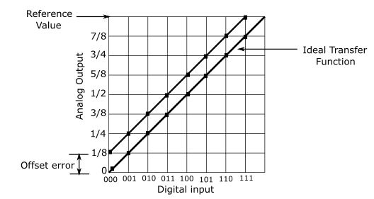
The offset error is measured by applying all input binary codes of logic 0s and measuring the output voltage then the deviation from zero output is termed as Offset error. The plot of transfer characteristics due to an offset error of 1 LSB is shown below in fig 2.
Gain Error
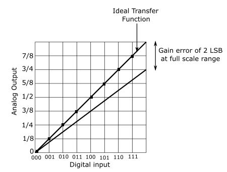
Gain error is defined as the difference between the calculated gain and the actual gain achieved. Gain error in percentage can be calculated by the formula given as
{\displaystyle\%\;gain\;error\;=\left(\frac{V_{11\;-}V_{os}}{V_{FS}}\right)\times100}
Where V11 is the output voltage, Vos is the offset error and VFS is the full range voltage.
Types of DAC
There are two ways to implement DAC through the resistive network. 1. Weighted Resistor DAC 2. R-2R ladder type DAC
Weighted Resistor DAC
The circuit of weighted resistor DAC has n electronic switches Dn, Dn-1,………..D2, D1 that is controlled by the binary input words. The switch makes a connection to the reference voltage(-VR ) for binary input 1 while it makes connections to the ground for binary input 0.
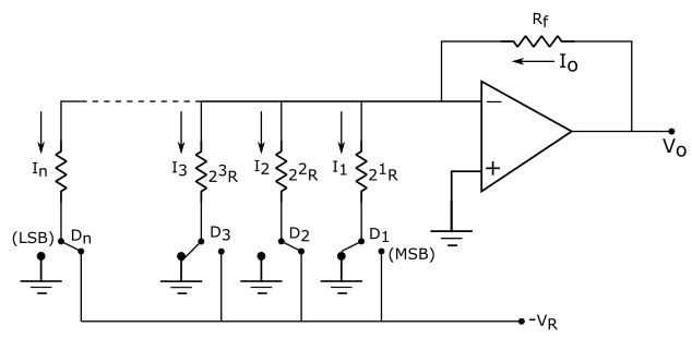
The output current of an ideal opamp can be given as
{\displaystyle I_{o}=I_{1}+I_2+I_{3}+......+I_n}
{\displaystyle \;\;\;=\;\frac{V_R}{2R}D_{1}+\frac{V_R}{2^2R}D_2+\frac{V_R}{2^3R}D_{3}+......+\frac{V_R}{2^nR}D_{n\;}}
{\displaystyle \;\;\;=\frac{V_R}R(D_{1}2^{-1}+D_22^{-2}+D_32^{-3}+.....+D_n2^{-n})}
The output voltage is given as
{\displaystyle V_o=I_{o}R_f=V_R\frac{R_f}R(D_{1}2^{-1}+D_22^{-2}+D_32^{-3}+....+D_n2^{-n})}
If Rf = R then
{\displaystyle V_o=V_R\frac{\cancel{R_f}}{\cancel R}(D_{1}2^{-1}+D_22^{-2}+D_32^{-3}+……+D_n2^{-n})}
{\displaystyle V_o=V_R(D_12^{-1}+D_22^{-2}+D_32^{-3}+...+D_n2^{-n})}
Advantage
- It is simple to construct
- Its cost is low
Disadvantage
- It requires many resistors of different values.
- The stability and accuracy of weighted resistor DAC depend on the accuracy of the resistors used.
R – 2R ladder DAC
R-2R ladder type DAC requires only two values of resistor i.e. R and 2R. Let us consider a 3 bit DAC in which the switch position D1, D2, D3 corresponds to binary word 100 as shown below:

As shown in the above fig, for the binary input of one, the switch connects the resistance to the reference voltage (-VR) and for binary input, the zero switches is connected to the ground. The equivalent circuit of Fig 5 for binary input 100 is shown below:
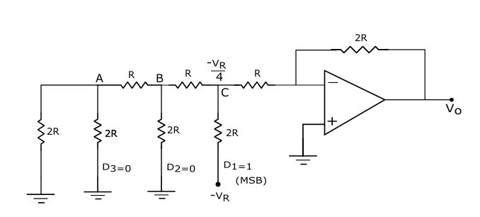
The voltage at node C is the input voltage to the inverting amplifier, so the node C voltage is calculated through the equivalent resistive network of fig 5 shown below

The voltage at node C calculated by the potential divider rule is given as
{\displaystyle \;\;V_c=\;\frac{-V_R\;\times\;\left(\frac23R\right)}{2R+{\displaystyle\frac23}R}\;\;\;=\;-\;\frac{V_R}4}The output voltage is given as
{\displaystyle \;\;V_c=\;-\frac{2R}R\;\left(-\;\frac{V_R}4\right)\;=\;\frac{V_R}2}So the analog output of R-2R ladder DAC for binary input 100 is VR/2
Advantage
- Only two types of resistor R and 2R are used
- Its accuracy is better than a weighted resistor network.
Disadvantage
Reference supply should be constant.
Analog to Digital converter(ADC)
Analog to digital converter is a system that is used to convert Analog signals into Digital signals.
Types of ADC
ADC are classified in the following ways:
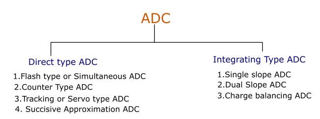
Direct type ADC.
The direct type ADC compares the given analog signal with the internally generated equivalent signal and produces the corresponding digital output. The various direct type of ADC is explained below.
Flash type or Parallel comparator ADC
It is the faster and most expensive comparator. To construct an n-bit flash type comparator, we need a 2n-1 comparator. To understand the operation of Flash type ADC, let us consider a 3-bit ADC as shown below:
Circuit diagram of Flash type Comparator
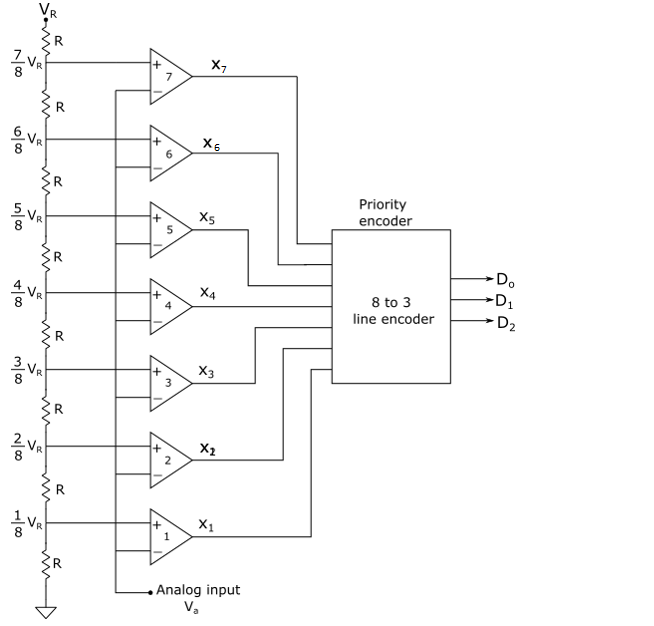
Working of Flash type ADC
The parallel comparator uses many comparators and the task of the comparator is to compare its both input and produce the corresponding output as summarized below in the table:
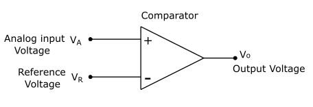
| Condition of input voltage | Logic output voltage (Vo) |
| VA > VR | Vo = 1 |
| VA < VR | Vo = 0 |
| VA = VR | Previous value |
The Analog input voltage Va is applied to each comparator’s positive(+) terminal. The negative (-)terminal of each comparator is connected to the different reference voltages that have been derived from the voltage source VR by using a resistive divider. The comparator compares the analog voltage Va with the corresponding node reference voltage and produces the logical output as shown in the truth table below:
The truth table of 3-bit flash type ADC
| Input Voltage | Comparator output | Encoder Output |
| Va | X7 X6 X5 X4 X3 X2 X1 | D2 D1 D0 |
| 0 to VR/8 | 0 0 0 0 0 0 0 | 0 0 0 |
| VR/8 to 2VR/8 | 0 0 0 0 0 0 1 | 0 0 1 |
| 2VR/8 to 3VR/8 | 0 0 0 0 0 1 1 | 0 1 0 |
| 3VR/8 to 4VR/8 | 0 0 0 0 1 1 1 | 0 1 1 |
| 4VR/8 to 5VR/8 | 0 0 0 1 1 1 1 | 1 0 0 |
| 5VR/8 to 6VR/8 | 0 0 1 1 1 1 1 | 1 0 1 |
| 6VR/8 to 7VR/8 | 0 1 1 1 1 1 1 | 1 1 0 |
| 7VR/8 to VR | 1 1 1 1 1 1 1 | 1 1 1 |
Recommended Articles

